
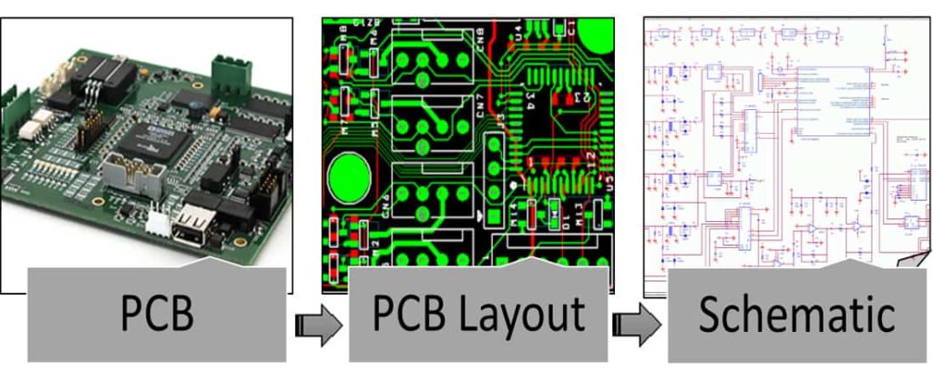
![Complete Guide: How To Do PCB Reverse Engineering [Works Quickly]](https://top10pcb.com/wp-content/uploads/2019/10/pcb-revese-2-1-806x440.jpg)
Complete Guide: How To Do PCB Reverse Engineering [Works Quickly]
As a PCB engineer, whenever I see a novel electronic device, I can’t help studying its structure principle and trying to make some improvements on it, because it always inspires me to improve my PCB DESIGN and seize the marketing opportunity. In fact, the purpose is to get a higher salary by great technical advantages, and PCB Reverse Engineering is the best way to achieve it. But how?
Do you think that 100% restore an electronic product is impossible? Well, although there are still some problems that cannot be solved in electronic engineering, it doesn’t include this. Basically, the only way to solve this problem is to rebuild the PCB CIRCUIT, scilicet reverse engineer the circuit board.
But how can we achieve this? How to complete Reverse Engineering? Don’t worry, sit back, relax, and learn.
What is PCB Reverse Engineering?
PCB Reverse Engineering, we usually call it PCB Clone or PCB Copy. It is a process to export the production files(Gerber File and BOM List)and designing files(Schematic and PCB file) of a particular printed circuit board by dissecting the electronic circuit and components so that we can help you replicate or improve the function of the board.
PCB reverse engineering is regarded as one of the most complex tasks in engineering science. Because this means restoring all the parameters and files needed for PCB production with little knowledge of a product.
Why Do We Reverse Engineer Circuit Boards?
Since it is so difficult and complex, why do we still stick to it?
That’s A Good Question.
We carry out reverse engineering of PCBs for a number of important reasons:
Replace obsolete components on the board
- Reposition certain components
- Enhance the functionality of the PCB
- Analyze and reinforce the security requirements
What Do You Need to Reverse Engineer a PCB?
Get Your Tools Ready
It’s going to be a long ride. The tools you need depend on the complexity of the project. If it is only a simple PCB, you can analyze the circuit with standard symbols by pencil and paper for easy understanding.
If the circuit is more complex, hardware and software designing tools are necessary. Like AutoTrace, Pstoedit, Dia, Gimp, and Inkscape.
Reverse Engineering Process
17 Steps to Reverse Engineering a PCB
#01:Getting Photos
Clean the board, at very least a quick brush with a paintbrush. Any specks of dirt, hairs etc will have to be removed in your photo editor if you don’t catch them now, and it there are many, this can be quite time-consuming.
If you have a tripod, and you can control the lighting, set everything up. You need to light the most boring picture ever. It also probably has to be quite close up, depending on the board. Select a plain background which gently contrasts with the board colour.
Take your time, set up the shot so that there is no perspective or as little as possible, and the frame is filled as much as possible. Use RAW mode if it is available, otherwise, just use the highest quality setting possible. Take pictures of both sides of the board, ensuring that the tracks are in focus. You may find it is better to photograph the board in sections and work on it a piece at a time.
Take a few pictures, with different settings, so you can choose the best ones.
If you don’t have a digital camera, you will have to scan your photo’s. Again, use the highest quality possible.
#02.Clean Up the Photos

Set up a directory for the project.I like to name the folder after the device I’m working on. Stick all the photos in there, and copy the ones you want to use into a sub-folder – I call mine “working”.
Start with the solder side of the board (although with SMD’s, there’s not going to be much solder there). Open the picture in the Gimp, and save-as something meaningful, like solder-side-clean.xcf, for example.
Flip the picture – otherwise, it won’t match the component side.
Set up a vertical guide. If the board has a ground-plane, align it to that, otherwise, just use the edge of the board or a long straight track. Rotate the image slightly so that the board or ground plane or track is aligned all the way down. (Of course, a horizontal guide may work better for you)
Set up a second vertical guide, and a pair of horizontal guides, aligned with the other edges (or ground-planes, or long tracks) of the board. Use the perspective tool (toolbox: right-hand edge, third tool down) and click each corner of the board you need to line up, and just drag them so that the other edges are parallel to the guides.
Make a rectangular selection around the board, invert it, and press delete. This will clear the background. Get rid of any other distractions like projecting connectors by selecting around them and deleting. Don’t mess about with the fuzzy select tool for things like this, just use the rectangle and ellipse tools. You can make compound selections/de-selections with these to make complex shapes.
Get rid of any artefacts using the clone and blur tools as appropriate. To use the Gimp’s clone tool, press ctrl when you click the area you are cloning from. A useful trick with vertical and horizontal PCB tracks is to set a guide over where you want to clone from and to.
The clone tool will snap to the guide. If you have tracks set at a 45-degree angle, rotate the layer (toolbox, 3rd row, 3rd tool along) by 45 degrees, and you can use the horizontal and vertical guides again. (You may have to enlarge the canvas to fit the picture) Rotate the board by -45 degrees to put it back how it was. Use the same trick for other known angles.
Okay, so you have a nice clean picture to work on. From now on, the general idea is that the picture contains a lot of detail, most of which you don’t want. The detail you want to keep needs to be separated out and kept as discreet images, so the next few steps concentrate on these two ideas.
Before you go any further, it is worth saving the image as a .png and opening it up in Inkscape. Click the image to select it, the go-to Path > Trace Bitmap… Experiment with all the methods and see if you can get an image where the edges of the tracks are nice and smooth, from that.
If not, at least you will get a good idea of what you are up against. If you get a clean image, work on it instead of the original. You still need to pick out holes and remove ground planes and substrate, but it should be much easier to work on due to having the edges of the tracks smoothed out.
Create a new layer, and make sure it is active. This will contain your alignment marks. Being on a separate layer, they will be easier to copy to the other layers.
Put borders at the corners of the board to make it easier to align the images later. To do this, make a square selection at each corner, then make another square selection the same size but shifted inwards a bit, using subtract mode. Fill the selection using the bucket fill tool. I didn’t do this and found alignment without corners to be tricky. You could use any alignment marks you like of course, corners is just what I thought of.
#03.Rescue the Holes

You need a picture of the holes/solder pads in the board to align the various images and make sense when you get rid of the holes later. This is especially important if you have taken pictures of sections of the board.
Depending on the individual circuit board, you may have to find a different technique that works for you.
It may be easiest to just paint them in. Create a new transparent layer (Layer > New Layer) and ensure it is active. Choose a brush about the same size as the pads, and dot over each one in some colour you like.
If the pads are copper coloured on a green board, as in the example, open the channels dialogue, and turn off the green and blue channels. With a little bit of luck, you will be looking at just the pads. If not, you have a bit more work to do – see the next paragraph for details. Go to Layer > New from Visible. Turn the blue and green channels back on.
Add a new layer and fill it with red, and change the red layer’s mode to Darken Only. You might want to repeat the process with another red layer. Delete any layers you are no longer using, such as the red layer(s) and the first New from Visible if you created more than one.
If turning off the green and blue channels did not make the holes/pads clear enough, go-to colours > components > decompose… Select HSV and click OK. When the new image appears, copy the “hue” layer and paste it as a new layer (edit > paste as > new layer) into the image you are working on. It should be the top layer. Set its mode to “subtract”.
With a bit of luck, you should now have clearly visible, if a bit dim, holes. Resume the procedure above. Again, the exact result will vary depending on the board you are working on. Try different decompose modes/layers if “hue” does not work you.
With the New from Visible layer active, use the select by the colour tool (toolbox, top row, second from right) to select the pads, adjusting the threshold as necessary. Copy the selection. Create a new transparent layer, set it active, and paste the selection. (You will need to “anchor floating selection” in the layers window). You can now delete everything except the layer with the holes/pads in it.
If this method does not work well for you, experiment with layers consisting of grayscale and inverted copies of the background, different coloured layers, turning channels on and off, and layer blend modes.
You may find that if the lighting is too uneven, you need to use one method on one part of the board, and a different method on another. Make a selection of the part you want to work on, create a new transparent layer, and paste the selection into it. All the parts will be visible through the transparency as you build up the layers. If you find all this is taking too much time, manually dotting the holes is probably quicker.
Find any bits of the track or other artefacts that are showing through and erase them. The dots that are left are now your place-holders for every through the connection on the board. Copy the alignment marks to the layer if you are using them, and save a copy to a new .png file. Call it something meaningful, like solder-side-holes.png. Finally, delete all the layers in the original file except the one showing the holes you rescued.
#04.Circle the Ground Plane Holes
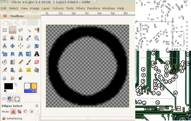
When it is used in the centre-line mode, Autotrace turns PCB trackpads into little loops. It is necessary, therefore, to remove them. Since we are going to delete the ground planes, some way of identifying where they are connected is necessary, so putting circles around them seems to be the way. There is a simple manual way to do this.
Create a new brush. Do this by creating a new image (File > New > height 64 width 64 > advanced options > fill with transparency).
- Elipse tool (toolbox top row second icon) and set its aspect ratio to fixed 1:1.
- Draw a circle in the new image so it fills the box exactly.
- Shrink the circle by about 5 pixels (Select > shrink)
- Stroke the circle (edit > stroke selection) – use a line of 7 or 8 pixels
- Save the file with the .gbr extension, in (for Linux users) ~/.gimp-2.6/brushes (the default export settings are fine).
- It’s worth doing a “+” and “x” brush whilst doing this – see next step.
- Restart the gimp.
Now open the file you are working on, and create a new transparent layer. Ensure you are working on this layer, and use your new brush (you will need to scale it) to dot a circle around every hole which is plated through the ground plane. Multiple or really awkward holes, you can draw a rectangle or free selection around, and stroke selection as you did to create the brush. Try not to overlap the edges.
Copy the alignment marks to the layer, turn off the visibility of everything except the circles you drew, save, and save a copy to a new .png file.
#05.Mark the Free Holes

A multi-layer board may have some pads which don’t look to be connected to anything. If so, they probably terminate some through plating which connects the other side of the board to an inner plane or track. You need to mark these “free” holes another way so you can relate them to the other side of the board later on. I have read that these inner layers are often used for ground and power planes, so shouldn’t be too hard to trace when you’ve done everything else.
Create another new brush in a cross shape – use the guides to help you. You may want to create an “x” shape and a “+” shape, which can interleave slightly.
Repeat the procedure you used to circle the ground-plane holes, only this time only put an x or a + over the free holes. This way, the centre of the mark still shows where the holes go.
I made these brushes by making triangular and rectangular selections on a 64-pixel square canvas, stroking them, then erasing the outer edges, however, I have since realised you could probably use a text “x” and “+”. Put a circle selection around the “x” the full width and height of the canvas, invert the selection, and delete the ends of the arms, so that it is not disproportionate to the “+”.
Copy the alignment marks to the layer, and save a copy to a new .png file.
#06. Remove Ground-planes

For the purposes of a schematic diagram, there is not much difference between ground-planes and the substrate. Since you marked the free holes and ground-plane holes you can also remove these.
Note that if you are dealing with a 4 layer PCB board, the internal layers are likely to be ground plane and power plane. Any through plated holes which do not connect to anything you can see is likely to be connected to a power plane, however, this is no way guaranteed to be the case, as there may be other traces hidden away in there. Hopefully, you will be able to work this out at the end with the aid of a continuity tester.
Use the fuzzy select tool to select each ground plane area. You can also fuzzy de-select, fuzzy add-selection and fuzzy intersect-selection. If fuzzy select is too uneven, use the circle, rectangle and free selection tools. It’s easiest to use the free selection tool by creating a series of straight lines by clicking and moving.
When you click the first spot again, it will close the selection. Before then, you can click and move any of the points you selected already. You can also draw freehand with it, though I find this too uneven. Grow the selection by one or two pixels (more if you have wide gaps between the tracks) to ensure there are no missed bits – this will also clean up the edges a bit (Select > Grow) and save the selection to a channel in case you need it again (for example, if you have to start over). Make sure you don’t pinch out any bits of track, though. Press delete to clear the selection.
Repeat for each ground plane area and the free holes, until they are all clear.
#07.Painted Areas

I found large painted areas to be the most problematic to deal with.
First, you need a way to see through the paint.
Copy the image to a new layer, and desaturate it. Choose luminosity. You will probably see a fair bit of detail already. You can bring this out a bit more by changing the layer’s blend mode – I found “burn” to be particularly good. Adjust the layer’s lightness (Colours > Hue-Saturation) to bring out more detail (this is more effective than using brightness/contrast).
Ensure the layer you are actually working on is active, and select any painted ground plane and substrate areas you want to remove. Save the selections to a channel, and delete them. You may also be able to use the clone tool to paint tracks over these areas, however, be careful not to paint in tracks that aren’t there!
I also discovered that a very clear, but somewhat rougher at the edges, view of the painted area detail can be obtained by decomposing to HSV (Colours > Components > Decompose > HSV) and viewing the saturation layer. It may be worth copying this to the main image as a layer, and experimenting with brightness, inversion, and modes.
You may find it easiest to make the selections for these areas by using the manual selection tools rather than the fuzzy select. I found it easiest to select the whole area, then isolate the bits I wanted to keep by de-selecting them. Always ensure the layer you are working on is selected, not whatever layer you are using to see the detail, otherwise, your hard work will be lost.
#08.Clean the Tracks

You are almost ready to process the image using AutoTrace!
You need the tracks to have good clean edges and smooth colour, or else AutoTrace will put in all sorts of details that you don’t want and probably didn’t even see since it traces a little bit too well.
I spent many, many hours trying to do this by selecting areas of track or substrate with the fuzzy select tool and using some method to smooth the edges.
If you are interested in reading a discussion about methods for doing this, please see this thread: http://registry.gimp.org/node/14912.
I found that any method that gave me something like a smooth edge also led to rounding off corners and pinched off-track ends. The idea was that I could then use the bucket fill tool to even out the tracks and substrate.
The best way to smooth out the unwanted detail is to trace the image using a different tracing program – I used Inkscape, which unfortunately doesn’t also offer centre line tracing. Some cleaning up still needs to be done first though.
Smooth out the fine detail using the selective gaussian blur tool (Filters > Blur > Selective Gaussian Blur). What this tool does is apply a blur which is limited, or “fenced in” by areas of high contrast. You can also use the wavelet decompose tool and delete the top (fine detail) layer, however, this may also remove details you want to keep.
I used a high radius of 30 pixels and a max delta of 29. These figures will likely be different for you. I found these by setting a very high blur radius, turning up the delta until all the detail disappeared, then turning it down again until I could see the tracks clearly, then turned down the blur radius to a saner level, judged from the sizes of the tracks in pixels.
Press OK. You should now find any “blockiness” in the tracks has been blurred out, but they are still clearly tracks.
Use the eyedropper tool (toolbox, 2nd-row 3rd icon from left) to pick an average colour from the remaining areas of the substrate. If the lighting is uneven, pick one of the lighter areas (probably not the lightest though). Set a few pixels spread for the eyedropper. This will set the foreground colour.
Create a new layer, setting it to be filled with the foreground colour, and move it below the layer you are working on. Most of the substrate should now be indistinguishable from the newly created background.
Create a new layer from visible. You should probably save this layer as a new image.
I found at this point I could see quite a bit of spread due to optical aberration at the edges of some of the tracks which were very close together, so I set guides along with them and used a small soft brush to paint background colour along these.
I also painted in the track holes in the track colour, but I’m not sure that this is necessary – it may be sufficient just to remove the dot of the actual hole in the middle.
Manually do any other cleaning up at this point. Don’t worry about light coloured marks on the actual tracks, or dark ones on the substrate, as these are going to get burned out.
#09.Reverse and Burn Out

You probably have light coloured tracks on a dark background. What auto trade needs is dark tracks on a light background.
Desaturate the image, that is to say, turn it into greyscale (Colours > Desaturate > Luminosity (or whichever works best)). Next, invert the image (Colours > Value Invert).
If you have a really clear, evenly lit, well-focused picture, this may be adequate, in which case you can go on to the next step. Otherwise, read on…
You need to burn out any detail on the background, which is now light grey or something approaching white, and “dark out” any detail on the tracks, which are now dark grey, or something approaching black. If the picture is badly lit, as mine was, this will by now be very obvious – but it just means you have to work in stages.
To do this, you need to set new black and white points for the image. If you have any area which is very different from the rest, isolate it with a large selection, feather the selection by a large amount (Select > Feather) such as 50 – 100 pixels, and work on it first, so it looks similar to the rest of the board.
Choose the levels dialogue (Colours > Levels). Near the bottom of the dialogue, there is a button marked “Auto” and 3 eye dropper buttons. The eyedroppers are to pick the black, grey and white levels.
Click the dropper for the white level, and click an area of the original substrate, if you can see any, which is a bit darker than the rest. Don’t use the darkest area as this may be too similar to the lightest track area.
Click the dropper for the black level, and click an area of the track which is lighter than the rest, if you can find any. Don’t use the lightest area as this may be too similar to the darkest substrate area.
Click OK. Repeat as often as you need to to get nice black or nearly black tracks on a nice white, or nearly white, background. Choose areas carefully to ensure that no tracks get blurred together or pinched through.
If you find that some area you did has become harsh and jaggedy at the edges, undo until it looks right again, and work on the remaining areas of the board by selecting and feathering as described above.
Paint in/out any unwanted details like writing, artefacts and the dots in the holes if you can see them. You may find some bits of track have become blurred together or pinched through – paint in repairs with a soft brush.
Copy the alignment marks to the layer, and save a copy to a new .png file.
#10.Smooth the Edges

You can try skipping this step, however, you may find that AutoTrace traces a bit too accurately, and you end up with a mass of fine lines. If that happens, you need to do the following.
The edges of the tracks will still look quite rough. The best way to clean them is to trace the image in a vector editor program such as Inkscape. The tracing can then be exported as a .png.
In Inkscape, open the file you made in the last step. Don’t worry about it fitting the page. Click the image to select it (black arrows will appear around it). Open the tracing dialogue (Path > Trace Bitmap). You may need to have a few goes at it. Try the defaults first before playing with the settings.
If you click the image, you will find you can drag the tracing and the original bitmap. Delete the original. The image you now have is made of vectors, which you can click and move around and deform individually. If you are unfamiliar with vectors, take the opportunity to have a play. You need a bitmap image to work with, so export the file (File > Export Bitmap). You’ll see a lot of scary-looking numbers, but you shouldn’t need to change anything except possibly the save directory and file name. Click “Export”.
Open the file in the Gimp and examine it carefully – you may find spots merged together or pinched off, and will need to paint in corrections to these.
#11.AutoTrace

This is what all the work so far has been leading up to. You are going to use AutoTrace to turn the collection of fixed lines, into a collection of moveable and connectible lines. These will become the lines of your initial schematic.
If you are using Linux, or some other ‘nix, for the files containing the tracks, run the following command:
autocracy -despeckle-level 5 -centerline -line-threshold 4 -output-format SVG -output-file filename.SVG filename.png
The important options are:
-centerline
-output-format
-output-filename
Note the American spelling, “centre”, of “centre”
I used the despeckle level setting for a file which hadn’t been first traced in Inkscape. If you included this extra tracing, you probably won’t need it (but it won’t hurt, either)
Sorry, I don’t know how this will look for a Windows user.
I suggest you read the manual page for this program, it has quite a few options to play with, and you should try running it with various alternatives. The important one to use, and the whole reason for using AutoTrace rather than the tracing tool in some GUI program, is the centerline option, which draws a single bezier line down the centre of each area, instead of tracing around it.
Open each attempt in Inkscape until you find something you are happy with. Delete all the attempts which you are not happy with. Record the version of the command you used, somewhere. Add a layer to the drawing, and paste into it the picture of the hole. Select the image of the holes and scale it so the dots line up with the ends of the tracks. Save the file. Use the break apart and snap together tools to fix any sections of track which have gone wrong. Save the file.
#12.Component Side

You should be pretty aux-fait with the methods now. However, with the component side, there is an additional layer of complexity, namely the components.
For an SMD board at least, the detail is too fine for manipulation of the entire image to be useful. So you need to do a lot by hand. You are likely to need the actual board to hand, and possibly a magnifying glass and continuity tester.
Open the picture you chose to use for the component side, and save it as a .xcf file with a meaningful name.
Open as a layer, the picture you created of all the holes.
Ensure the layer with the component side is selected, and use the scale, rotate and perspective tools to adjust it so that the holes you can see the line up with the holes you captured from the solder side. Chances are it won’t match exactly. My board is slightly bent, so the alignment was a little bit off in the middle.
You need to create a picture of the components, a picture of the tracks, and pictures which identify any “special” holes.
If you wish to isolate the component identifiers marked on the board, do so now. Click the little red square in the corner of the main image window to turn on the quick mask – the picture will fill up with transparent red. Paint white to erase the mask from the writing. Just do it in blocks, don’t try to follow the lines of the letters.
Toggling the quick mask (click the little square again) will turn the bits you painted into a selection, and copy to a new transparent layer. Use the “levels” technique described for making the tracks stand out, selecting the text and an area of track (assuming the tracks are lighter than the substrate) for the black and white points. Paint in any bits that get pinched off.
#13. Fill in the Substrate

In my picture, everything was a bit blurry, so I decided to paint in the substrate first. This leaves the tracks much easier to follow and the components better defined. Also, this helped clarify areas which were in shadow. With a sharper picture you could probably do this with the Bucket Fill tool, set to “fill similar colours”, but after I used this a few times I decided to make manual selections and fill those, which also conveniently obliterates the painted markings.
First of all, create a new transparent layer to work on.
As most of the substrate on my board is in square or rectangular sections, the method I used was to use the rectangle tool to select an area of substrate including pads and one or more components within it. Then I deselected the component, pads and tracks. I used the circle and free-select tools as necessary. I then used the bucket fill tool (set to “fill whole selection) to fill the area with black. Use the layer rotation trick with the guides to select diagonal areas.
You will have to save the selection to a channel if you do this, and clear it before rotating the layer. You can then turn the channel into a selection and rotate it to match. If you have a steady hand, you could paint in these areas with a brush tool.
Use the selection tools most appropriate to the board. Don’t worry about trimming edges off the tracks if they are a bit fuzzy, however, don’t be tempted to “edit” the board layout at this stage, as it may lead to confusion later on.
If you have a good picture, there may be no need to do this.
#14.Isolate the Components

You will eventually need to replace the components with their symbols, but for now, isolate them into an image of their own.
The easiest way to do this for SMD’s is with rectangle and circle select tools, however, you may find it better to use the quick mask and a brush tool described previously.
Invert the selection, copy it (ctrl-c) and paste it into a new transparent layer. Save this layer as a new .png file. Save the selection to a channel (in case you stuff things up) Delete the selection from the base image.
Try to work out where the tracks went that are hidden by the components, and paint them in using the same colour as the tracks you can see. This is where a continuity tester will prove useful. Find datasheets for the components, the sample circuits may help work out what goes where.
Use the guides to help you, and use the selection and bucket fill tools if you are not comfortable painting. Use the eyedropper tool with a small spread to select the colour. You may need to use a magnifying glass and the actual board to see where the tracks probably go.
Create a new black layer (since you filled the substrate with black) and place it behind the component layer. This should fill the spaces with black where the components were.
On my board, the component side also had considerable ground plane areas, which I deleted.
Optionally, use the levels technique previously described to turn the tracks into
#15.Combine the Sides

Fire up Inkscape and open the image of the component sidetracks. Create a new layer, and cut this image and paste it into the new layer. Create another new layer. Open the tracing you previously made of the solder side of the board, copy it, and paste it into the new layer. Close the tracing.
Create a new layer. Open the picture you made of the holes, copy it and paste it into the new layer, then close it. You may also want to repeat for the image of the components, the ground plane hole circles, the free-hole marks and the complete image of the component side if you want to use these for extra guides. I also added in an image of the solder side tracks to confirm that the first tracing was correct.
Open the layers dialogue and re-order the layers so the original photo is at the bottom, then the picture of the components, then the component sidetracks, then the holes, then the tracing. Use the scaling arrows for each layer (click to select the image) to adjust it so they are all aligned. Use the holes to guide you. You may need to set the aspect ratio to “free” for tweaking.
Adjust the transparency of the layers so you have an image showing what is connected where.
Using the bezier tool, trace a line for each track. This will be easier if you filled in the substrate earlier. Click every time you want to change direction – this will add a node to the line. Double click to finish the line.
You will probably want to turn on or off the other image layers as you work to check your progress and to check the “sanity” of your tracing.
You need to combine the two tracings. Go to Edit > Select All in All Layers, then Path > Combine. This will let you now select multiple paths. Go to Edit > Deselect.
Inkscape provides a tool to snap together the ends of lines. Use the edit tool. For every place, you find where a track on the top of the board connects through to a track on the bottom of the board, select the connector on the end of one, press shift and click the end of the other. They should both have big coloured nodes on the end when selected.
Then click the snap together icon. Any track ends you have leftover most probably connect to a ground plane or an internal plane which may be either ground, power or a section of track. Use the other layers to help you investigate any which don’t correspond to anything.
Finally, delete all the layers except the tracing. Save the file as postscript (.ps) The reason for this is that Dia has a problem importing .svg format files (hopefully to be fixed in version 0.98) and an intermediate step is needed to generate a format it can use, in this case, the xfig format, .fig.
#16. Add Component Symbols

Use the pstoedit program with the options:
pstoedit -f fig inputfile.ps outputfile.fig
It is possible to generate a schematic format output file, but I found this hard to add components to.
Use Dia to open the .fig file you just made. Dia is a great little program which has an excellent range of objects which can be snapped to lines. A bit like MS Autoshapes, only much better.
If you have used Visio, you should be comfortable with Dia. Choose the “Circuit” category of shapes. Using the image of the components as a guide, snap-in symbols to replace them. Visit the Dia website for extra symbols in the “Electronic” and “Circuit 2” categories. (Others may exist, I just haven’t found them)
I used the lamp symbol to represent unknown connections – ie those which are connected to a “free” hole on the solder side. These can later be filled with corresponding colours.
Dia has a text tool. If you snap text to a shape, it will move with the shape. You can attach it to lines where you see a connection point. You probably want to add values and/or identifiers this way.
Creating a new symbol with Dia is also a good choice. Create the symbol as a diagram, then export it as a .shape file. The files are easily editable in a text editor to remove surplus connection points and tweak line positions.
The majority of datasheets for chips and transistors can be found on the internet, though you may have to dig somewhat. Create “mystery box” symbols for any mystery devices. You may be able to work out what they are once you have rearranged the drawing into a schematic.
#17. Finally, Rearrange

All being well, you should now have a vector drawing of all the tracks, with symbols added. The wonderful thing about vectors is that you can move them around, and this is how you are going to turn what is still really a picture of the tracks on the board, into a schematic.
Chances are the circuit board layout bears at least some relationship to the original schematic, so bear this in mind as you move things around.
Start by moving obvious groups of components into areas with a bit of space around them. Optionally, replace the lines you traced with zigzag lines. These are composed exclusively of vertical and horizontal sections and are ideal for this purpose.
If you are used to circuit diagrams having a dot to represent connections, you have the choice of putting in extra lines to accommodate these, or using the more modern style of not using them.
In this case, crossed lines are only crossed, not connected. If a connection is represented, they are offset.
Arrange the components in each group so it looks more like a sensible schematic.
Work your way through the drawing, pulling out components and replacing lines as you go.
Arrange on a more general scale so that most of the connections between groups are in “sane” positions – ie, not too much crossing over, not too many going from one side of the drawing to the other.
When you are happy with the positions of everything, remove the excess points from each line, and sharpen the corners.
Study the power routing through the circuit to check the sanity of assumed VCC (or vdd) connections. Compare to the actual circuit board with a multimeter to check. Check any “probable” inner layer tracks.
Remember, some of the tracks which were connected on both sides of the board may also be connected to a plane or track sandwiched inside the board. If there are obvious peculiarities in the circuit, it may be because such a connection is hidden from you, and therefore missed.
Conclusion
Pcb reverse engineering is not only a process of copy, but a good way to learn from excellent design solutions, improve professional skills, and develop better new products.
PCB reverse engineering is of great difficulty for a beginner, so why not ask our experienced engineering team for help.
Contact us for any questions and welcome all the comments.
Comments ( 2 )
[…] circuit diagram can provide information about how the individual components must be connected provide specific […]
[…] determined circuit board size and various mechanical positioning, draw the PCB board frame in the PCB design environment, and place the required connectors, buttons/switches, screw holes, mounting holes, etc. according […]