PCB Anti-interference Design Techniques Tutorial
The anti-interference problem is a very important link in modern circuit design. It directly reflects the performance and reliability of the entire system. For PCB engineers, the anti-interference design is the focus and difficulty that everyone must master. It not only directly affects the reliability of electronic products, and the stability of the product. Even the success or failure of the PCB design.
Interference Problems in PCB Boards
In actual research, it is found that there are four main interferences in the PCB circuit design. Power supply noise, transmission line interference, coupling, and electromagnetic interference (EMI). Let’s take a closer look.
1.Power Supply Noise
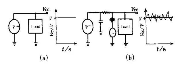
In high-frequency circuits, the noise of the power supply has a particularly significant effect on high-frequency signals. Therefore, firstly, the power supply is required to be low noise. Here, clean ground and clean power are equally important.
2.Transmission Lines
There are only two types of transmission lines that can appear in PCB circuit boards: strip lines and microwave lines. The biggest problem with transmission lines is reflection. Reflection causes many problems. For example, the load signal will be the superposition of the original signal and the echo signal. Difficulty in signal analysis; reflections can cause return loss (return loss), which affects the signal as much as it does with additive noise.
3.Coupling
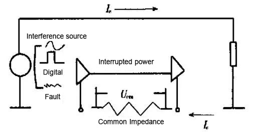
The interference signal generated by the interference source is electromagnetic interference to the electronic control system through a certain coupling channel.
The coupling mode of interference is nothing more than acting on the electric control system through wires, spaces, public lines, etc.
There are mainly the following types of analysis: direct coupling, common impedance coupling, capacitive coupling, electromagnetic induction coupling, radiation coupling, etc.
4.Electromagnetic interference (EMI)
There are two types of electromagnetic interference: conducted interference and radiated interference. Conducted interference refers to the coupling (interference) of signals on one electrical network to another electrical network through a conductive medium.
Radiated interference refers to the interference source coupling (interfering) its signal to another electrical network through space. In the design of high-speed PCBs and systems, high-frequency signal lines, integrated circuit pins, and various connectors can all become antenna interference radiation sources, which can emit electromagnetic waves and affect other systems or other subsystems in the system normal work.
PCB and Circuit Anti-interference Measures
The anti-interference design of printed circuit boards is closely related to the specific circuit. Next, we will only explain a few common measures for PCB anti-interference design.
1.Power Cord Design
- According to the current of the printed circuit board, try to increase the width of the power line to reduce the loop resistance.
- Make the direction of the power line and the ground line consistent with the direction of data transmission, which will help to enhance the anti-noise capability.
- Connect the 10 ~ 100μF decoupling capacitor to the PCB power input terminal.
2.Ground Wire Design Principles
- Separate the digital ground and analog ground. If there are both logic and linear circuits on the board, they should be separated as much as possible. The ground of low-frequency circuits should be grounded in a single point in parallel as much as possible. When the actual wiring is difficult, it can be partially connected in series and then grounded in parallel. Ground high-frequency circuits in multiple points in series. The ground wire should be short and leased. Use grid-like large-area ground foils around high-frequency components as much as possible.
- The grounding wire should be as thick as possible. If the ground wire is a very straight line, the ground potential changes with the change of current, which reduces the anti-noise performance. Therefore, thicken the ground wire so that it can pass three times the allowable current on the printed board. If possible, the ground wire should be above 2 ~ 3mm.
- The ground wire forms a closed loop. The ground wire should form an endless loop as much as possible, which can reduce the point difference of the ground wire. Most of the printed circuit boards composed of digital circuits, the grounding circuit of the printed circuit can improve the anti-noise ability.
3.Configuration of decoupling capacitors
One of the common practices in PCB circuit design is to configure appropriate decoupling capacitors in various key parts of the printed board. The general configuration principles of the back-off capacitor are:
- Connect the input end of the power supply across an electrolytic capacitor of 10 ~ 100uf. If possible, it is better to connect above 100uF.
- In principle, each integrated circuit chip should equip with a 0.01pF ceramic capacitor. If the printed board has insufficient space, a 1 ~ 10pF capacitor can be arranged for every 4 ~ 8 chips.
- For devices with weak anti-noise capability and large power change during the shutdown. Such as RAM and ROM storage devices, a decoupling capacitor should be directly connected between the chip’s power line and a ground line.
- The lead of the capacitor should not be too long, especially the high-frequency bypass capacitor should not have the lead.
- Equipped with a 0.01μF decoupling capacitor on the reset terminal “RESET” of the one-chip computer.
4.Methods for Eliminating Electromagnetic Interference in PCB Design
- Reducing loops: Each loop is equivalent to an antenna. So we need to minimize the number of loops, the area of the loop, and the antenna effect of the loop. Make sure that the signal has only one loop path at any two points, avoid artificial loops, and use the power plane as much as possible.
- Filtering: We can use filtering to reduce EMI on power lines and signal lines. There are three methods: decoupling capacitors, EMI filters, and magnetic components.
- Shielding.
- Minimize the speed of high-frequency devices.
- Increasing the dielectric constant of the PCB board can prevent high-frequency parts such as transmission lines near the board from radiating outward; increasing the thickness of the PCB board and minimizing the thickness of the microstrip line can prevent the overflow of electromagnetic lines and prevent radiation.
5.Proper Use of Anti-jamming Devices
- When designing the electromagnetic compatibility of PCB, according to the different characteristics of noise, correct selection of anti-jamming devices: absorb the surge voltage with diodes and varistor, isolate power supply noise with an isolation transformer, etc., and filter out certain frequency bands with line filters, etc. The interference signal is bypassed, absorbed, isolated, filtered out, decoupled, etc. with a combination of resistors, capacitors, inductors and other components. If the anti-jamming device is not in proper use, it will not only effectively reduce the interference but also become a new source of interference.
- For the selection and installation of capacitors, tantalum electrolytic capacitors are effective in low-frequency applications and should be installed at the power inlet; Ceramic capacitors are effective in high-frequency applications, install them near various integrated circuits. When installing a capacitor, you must shorten the lead as much as possible. But you cannot ignore the installation position for the sake of short lead. It should be installed near the Vcc and GND pins of the integrated circuit that needs to be bypassed. Otherwise, the capacitor is meaningless. When the impedance of the signal wires on the board does not match, reflected noise will occur multiple times. To eliminate interference, connect impedance matching resistors at the line terminal and the beginning. When the printed wire is long, the line inductance will cause amplitude reduction oscillation, which will be damped in series, which can suppress the oscillation, enhance the anti-interference ability, and improve the waveform.
6.Reasonable PCB Layout
Improper device layout on the PCB is also an important factor that causes interference. Therefore, in the component layout, fully considers the circuit structure and arrange the components on the printed circuit board reasonable.
(1) Reasonably determine the size and shape of the PCB
If the PCB size is too large, the wires will be lengthened, the impedance will increase. And the noise margin will be reduced. If the size is too small, it will not be conducive to heat dissipation. The adjacent wires and devices are prone to interference.
(2) Reasonable arrangement of components
- Arrange the input and output sections on each end of the board
- The interconnected devices in the circuit should be as close as possible to reduce the distance between the connecting wires between the devices
- Configure components around the core device to minimize the lead length
- Devices with close working frequency or a large difference in working-level should be far away to avoid mutual interference
Example
For a small-scale development system circuit with a single-chip microcomputer as the core. When designing a printed circuit board, it is advisable to place clock-producing devices, oscillators, and other noise-prone components close to each other. Keep related logic circuits as far away as possible Noise devices.
At the same time, considering the installation method of the circuit board in the cabinet. It is better to arrange ROM, RAM, power output devices, and power supplies that are easy to generate heat on the edge or upper part of the board to facilitate heat dissipation.
Conclusion
In general, using the above basic anti-interference measures can eliminate about 90% of common interference on PCBs. If you want to eliminate some special, small-probability interference, you must use special, more complex hardware anti-interference circuits.
However, excessive use of hardware anti-interference design measures will significantly increase the conventional cost of the product. And the increase in the amount of hardware will also generate new interference, which will cause the reliability of the system to decrease.
Therefore, according to the design conditions and target requirements, we should adopt some hardware anti-interference measures reasonably to improve the anti-interference ability of the system.
Comment ( 1 )
Good article! It’s very helpful for a beginner technical engineer like me. I always face some technical problems in PCB anti-interference design. I don’t know how to design the circuit diagram to achieve the best performance. Now I can debug it in your way.
Looking forward to more practical technical guidance articles like this.